A brief history of the QUUB design
I've been looking through some old designs and realised that it's been over 10 years since I had the first idea to design the QUUB, I can't believe that.
So I thought it would be interesting to provide a (very) brief history of the design.
Let's start with an early version, I'm not sure if this was the first but it certainly was at least close to the first.

I guess this is about as weird as it gets, the stackplane is a core of connections in the center of the PCB, and dockables are triangular in shape, there being four possible at each stack level.
Four dockables in place.
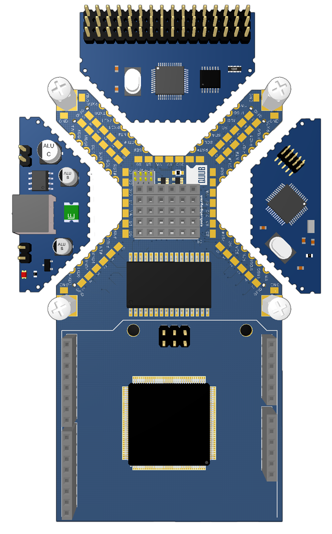
The next image shows an exploded view, note the bottom dockable, that was designed to host an Arduino Due and a 256k RAM.
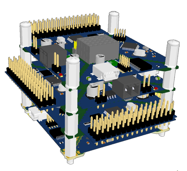
Four stackables connected, you can now get where the "stack" terminology came from.
And finally the track layout.
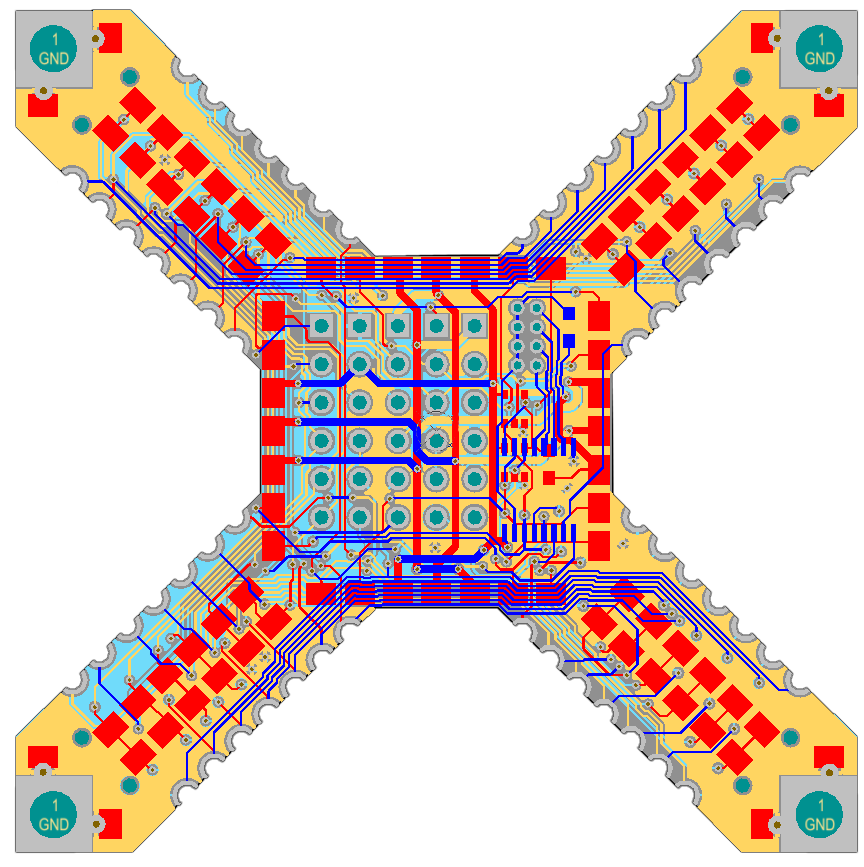
This design was never built.
Next we have a design based on the ATMEGA 2560.
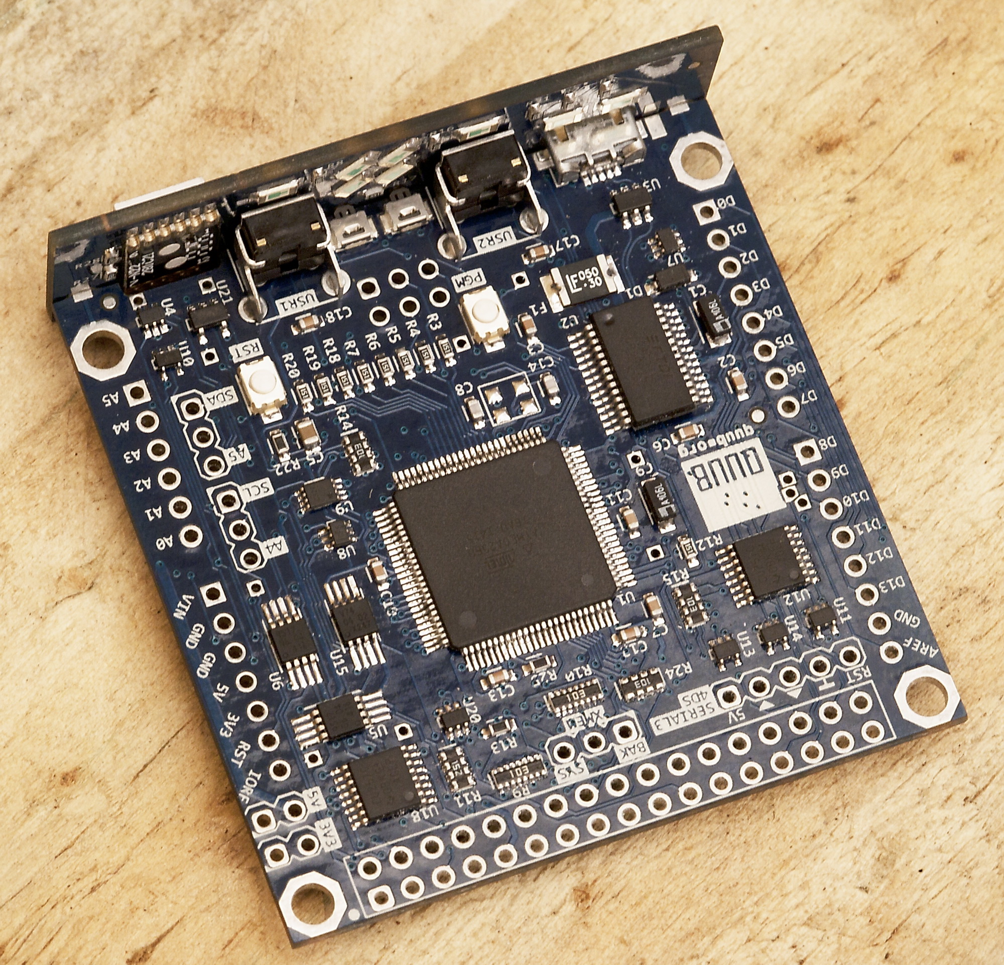
Note the provision for socket strips that mechanically match the Arduino standard, this was going to be an Arduino-Mega compatible board with a lot of extra features.
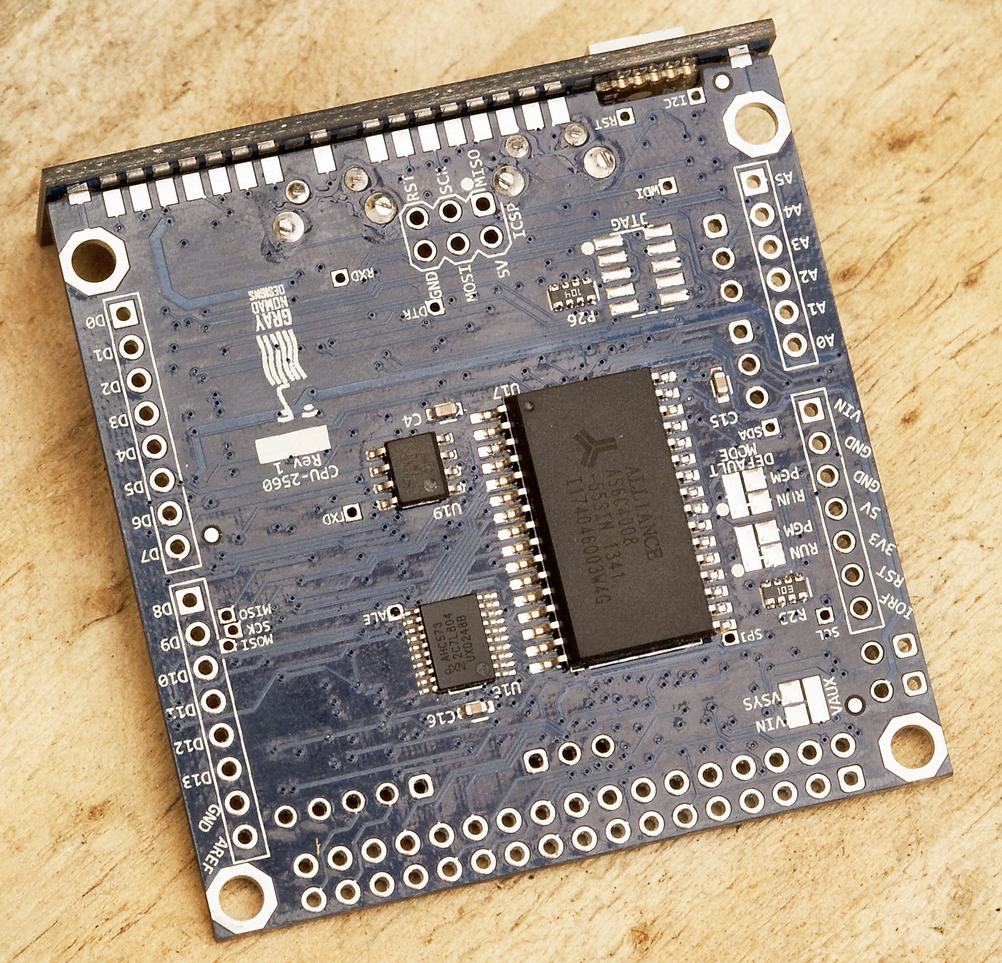
This is the reverse side showing a 256k RAM and some other control logic.
One feature of this earlier design was the ability to solder a front panel directly to the PCB.
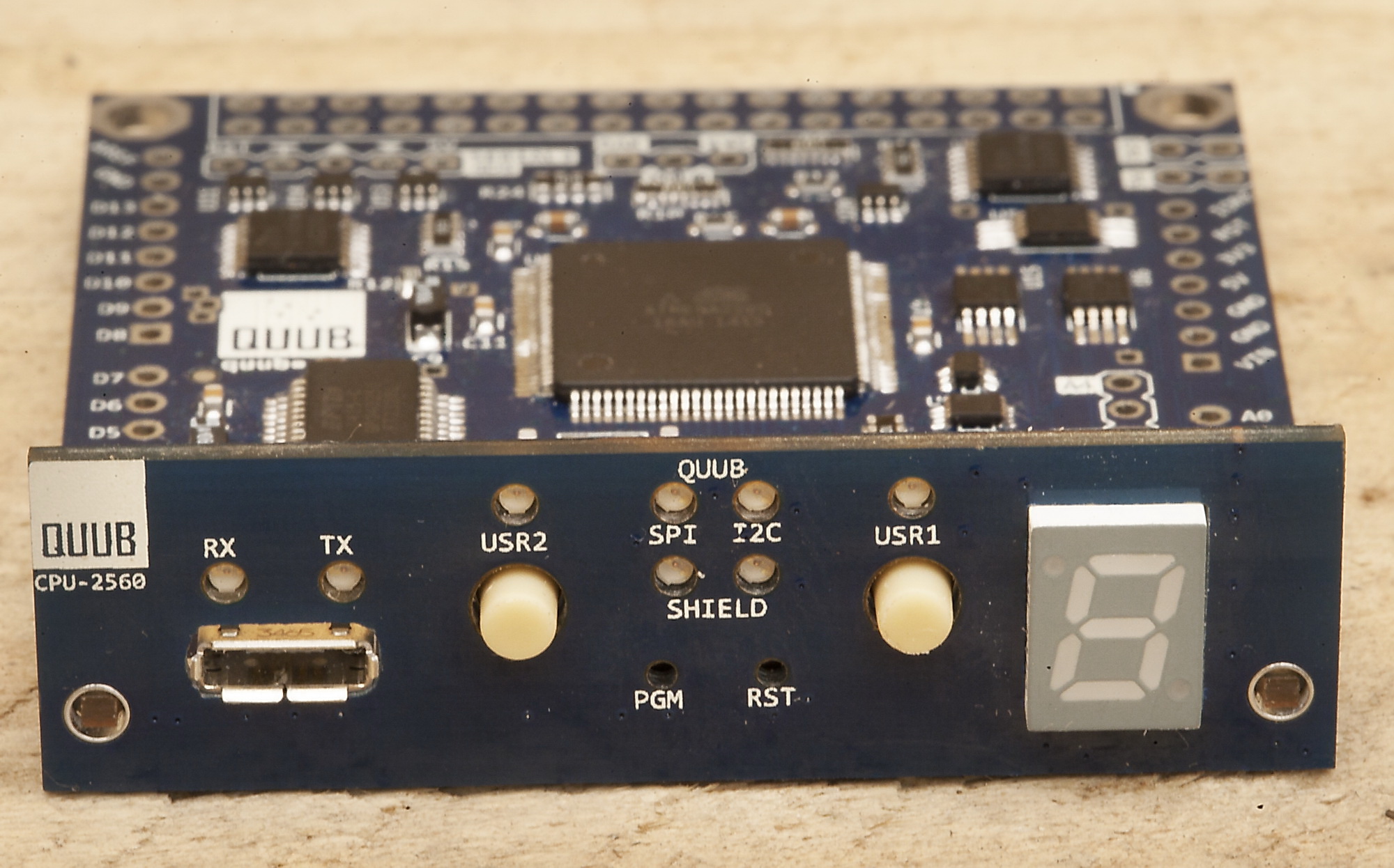
This panel had access to just a few signals for LEDs etc but had cutouts to allow switches etc to protrude. Later designs had all the stackplane signals available on all sides so up to four panels could be soldered on to create a "self enclosing" design and all sides could host any manner of logic and/or IO.
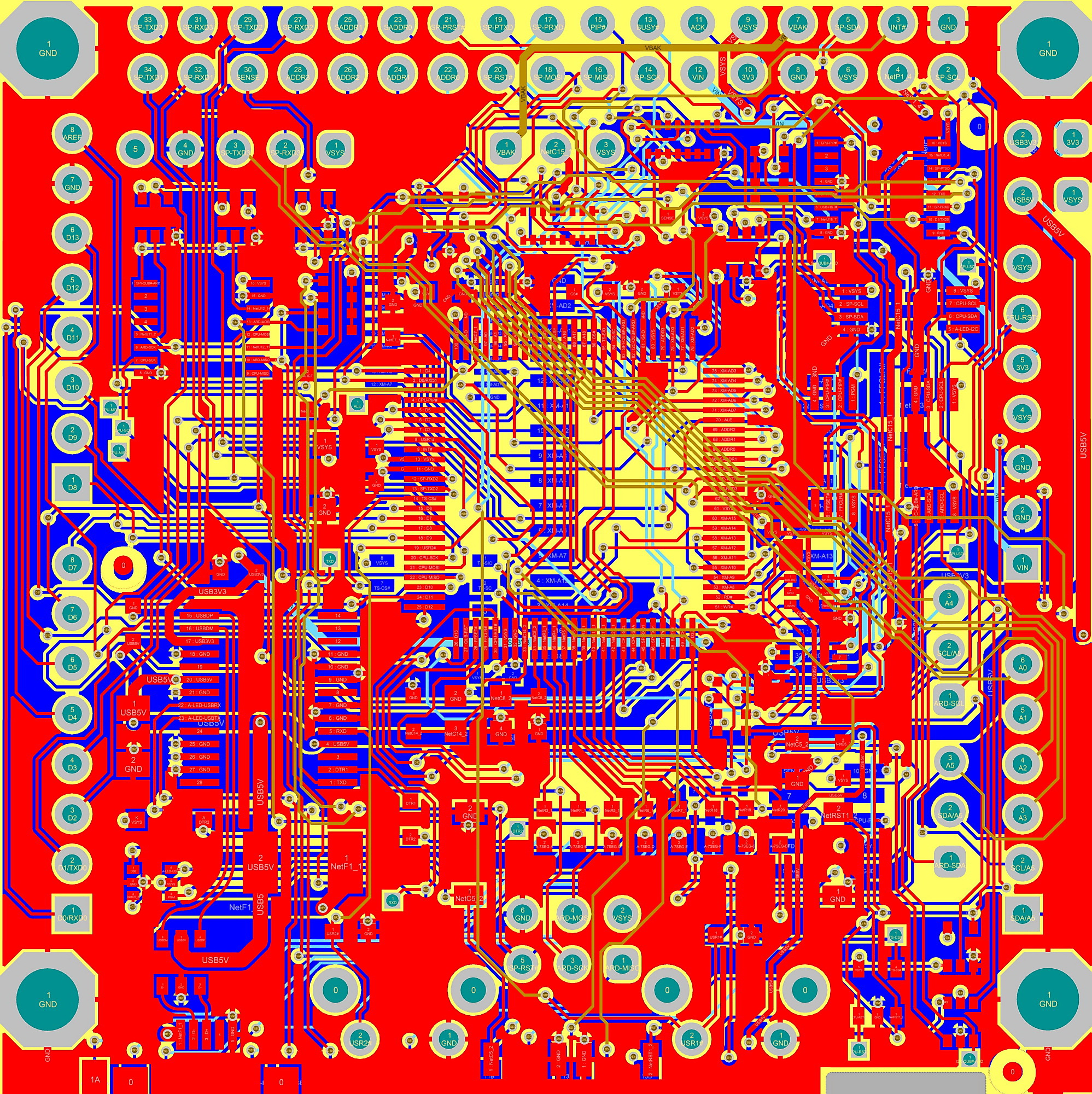
Here we see the track layout for this board. In those days I refused to allow any signals on the inner two layers (I always use a 4-layer PCB) as I considered that they were reserved for power planes. So this board took some time to lay out (I don't use auto routing)
Skip foward a few years and we have this much simpler design.
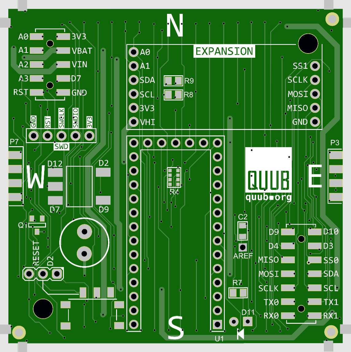
By now it's getting too hard to bootstrap a modern MCU from the ground up and anyway you can buy tiny proto boards for $5 or $10 so why bother. So this design used an Itsy Bitsy board as the MCU.
The Isty Bitsy board used here has a SAM D51 processor which is quite powerful but not a lot of IO.
This board was never fabricated but it's immediate successor was...
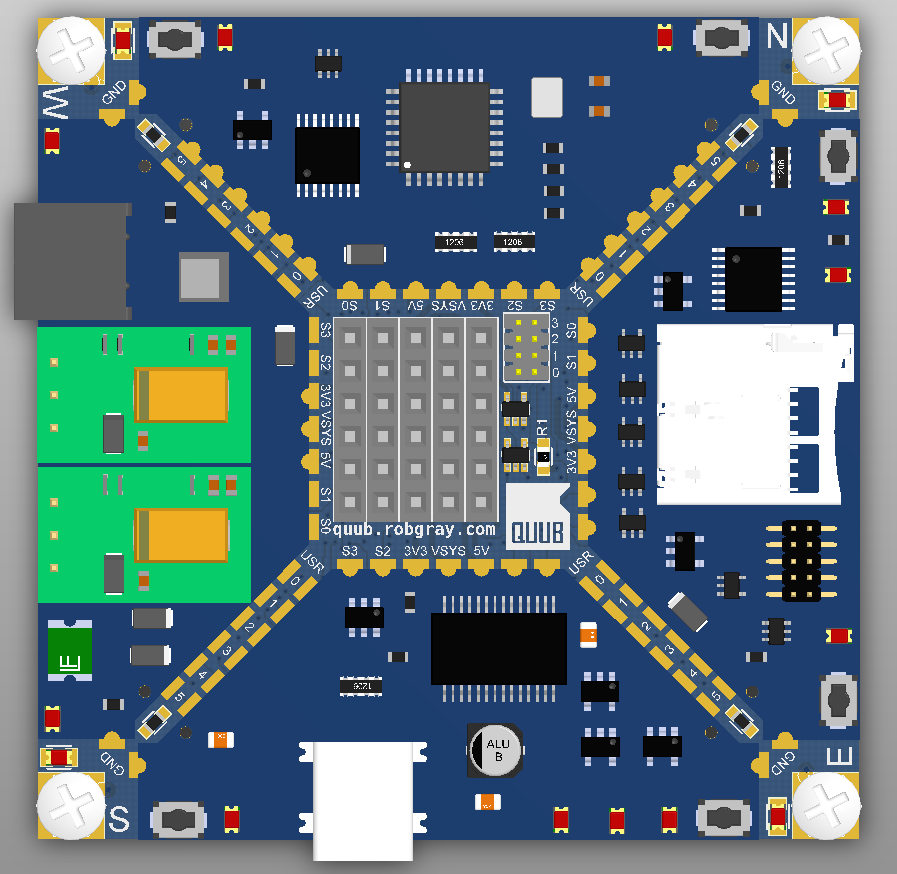
...this board.
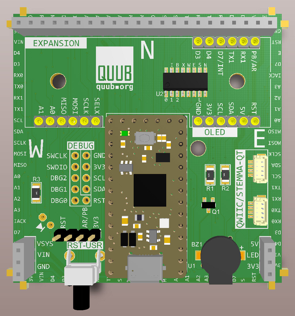
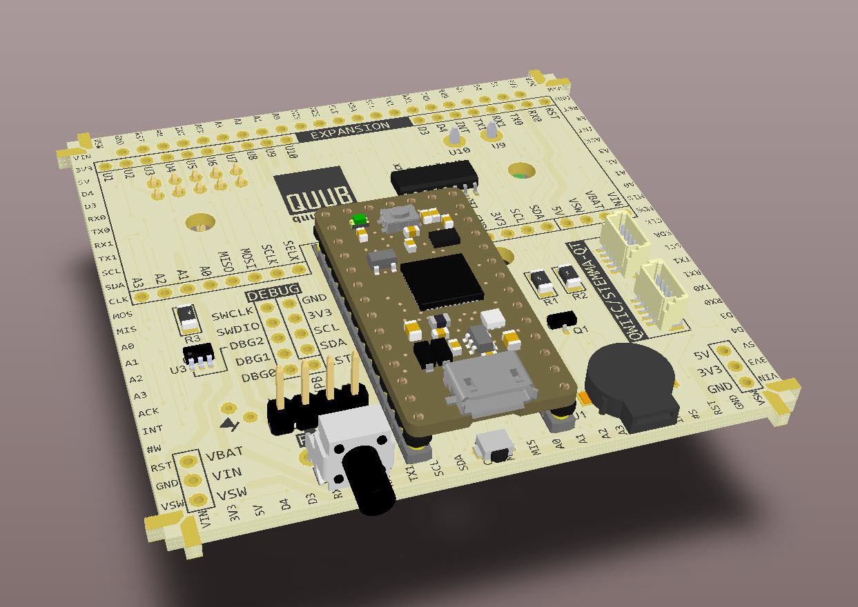
We're getting more recent now, maybe around 2020 and I did actually have these PCBs fabbed.
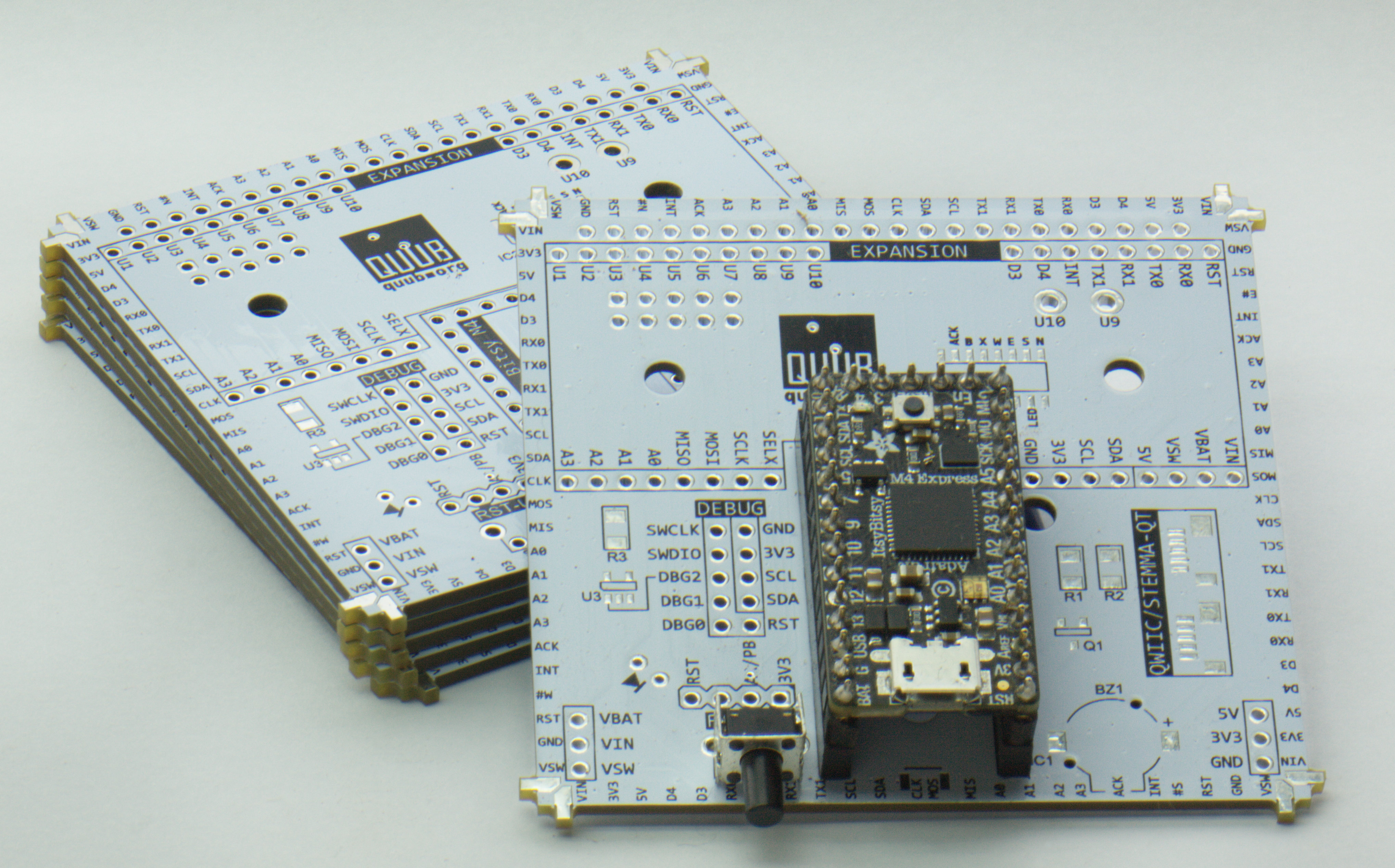
Note the signals marked on each edge and and the tabs on each corner. These were for the side panels I mentioned ealier.
And then I discovered the Raspberry Pi Pico, finally an MCU board with castellated pads that will allow me to solder it directly to my host board. So yet another design was called for.
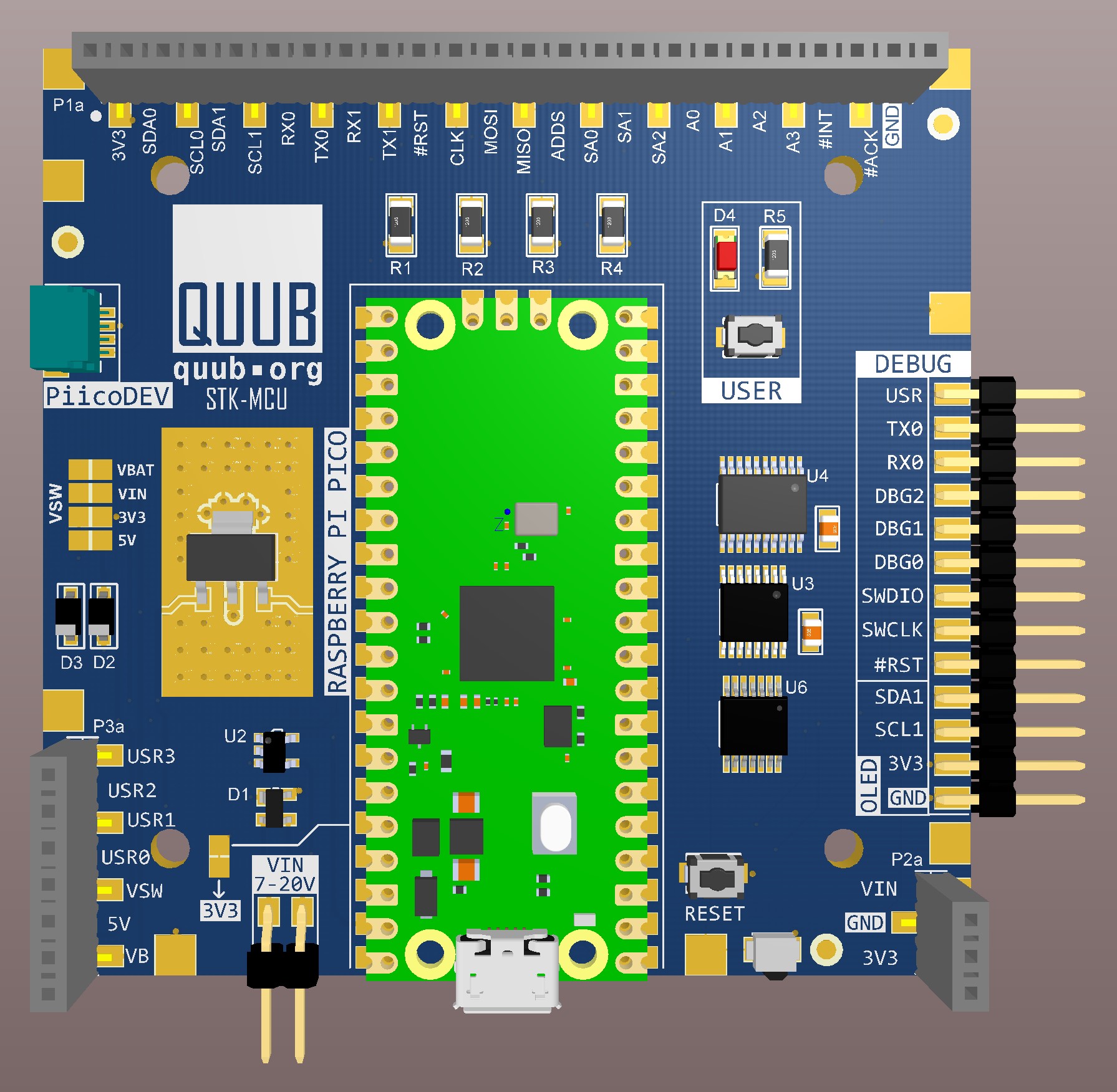
I also reasoned that the Pico has a much larger following and better support than the Itsy range, so that was a consideration as well.
This stack of boards shows where the QUUB name came from.
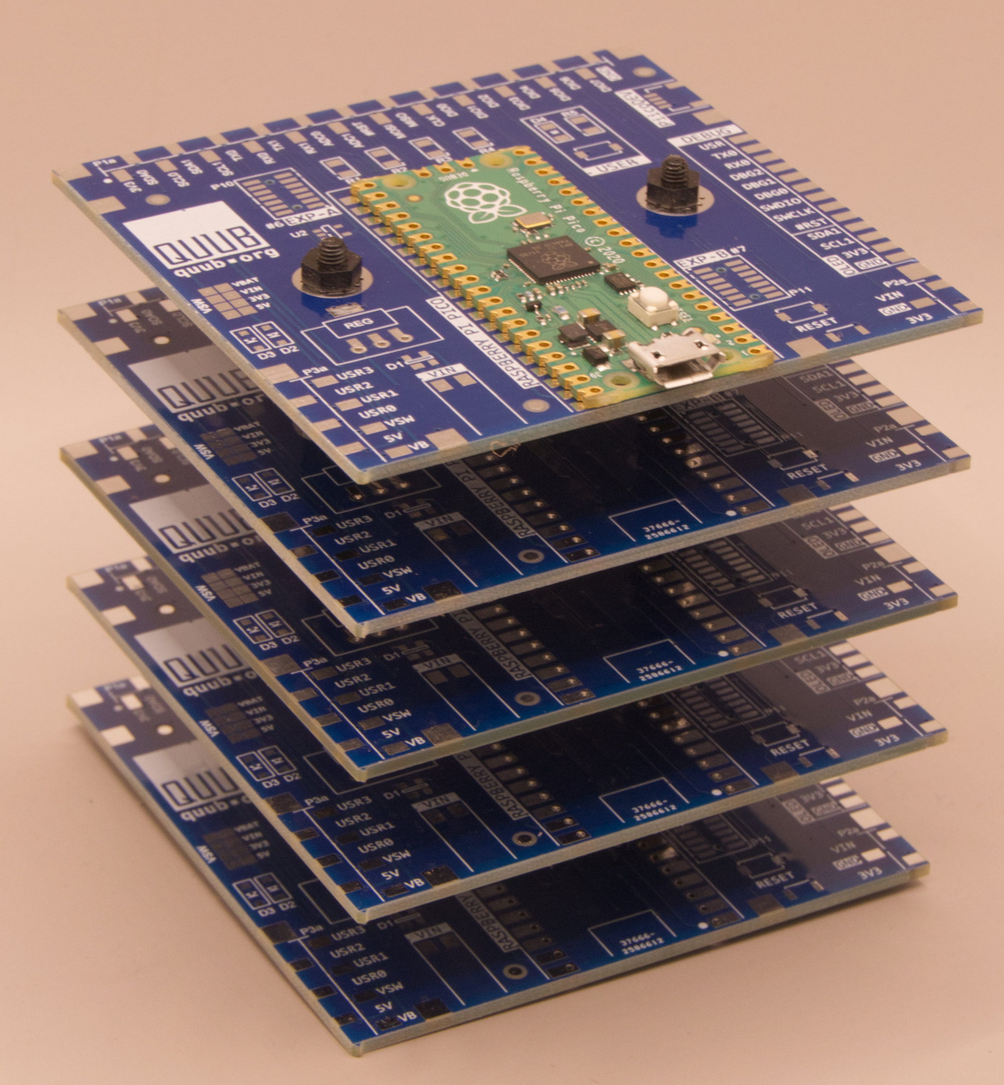
However this was to be the last of the square QUUB designs.
Then I started adding more and more IO and the design started physically growing to accommodate the extra components.
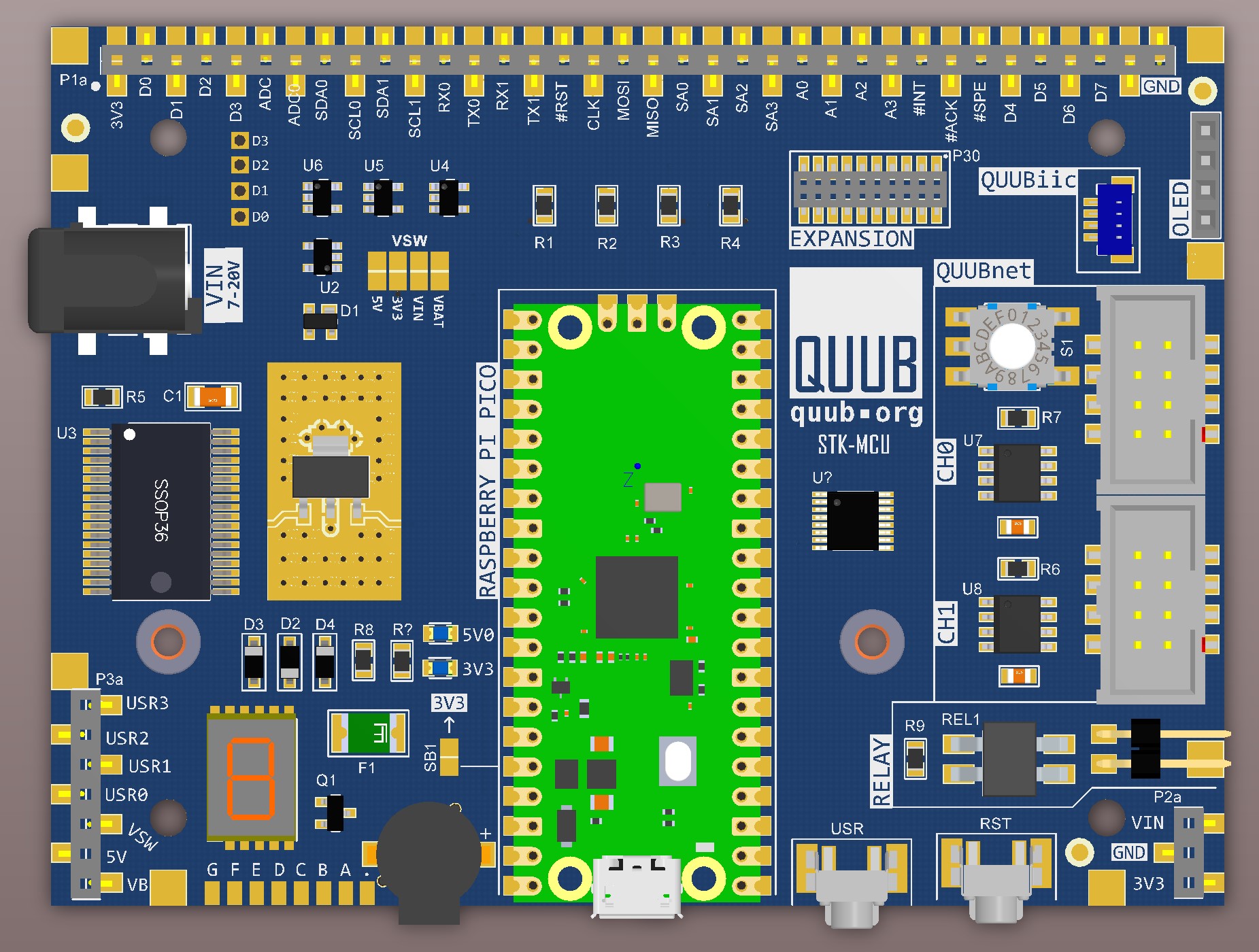
We are now losing the QUUBish square look, this was a big decision on my part as that square format had been fundamental to the entire idea for years. But no point getting too hung up on an idea eh?
So once that Rubicon had been crossed all bets were off and the board just got larger and larger with all sorts of features hard-coded into it.
Eventually however I decided that it did not make sense to include such things as the power supply and QUUBnet hardware into the base design. What if an application needed a different PSU to handle higher voltages, and just how many applications will really need the QUUBnet to talk between multiple stacks?
So a design was made that outsourced most of those features to small add-on boards.
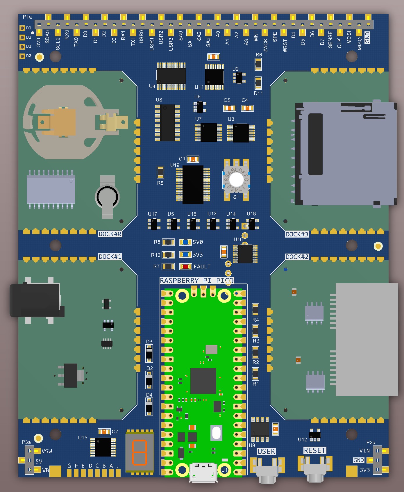
We are almost there. This design had four docks for add-on boards and in the above example we have a PSU, RTC, SD card and dual RS485 ports, which is great and maybe just what one needs for a data logging application, but where does the data come from? There are no more docks for sensor IO and while you can stack another board or two (or 15 if you like) what if just a single I2C bus would allow you talk to multiple sensors and thus complete the application on a single board.
So I added another two docks and provision for a remote dock, and the result is the current QUUB design.
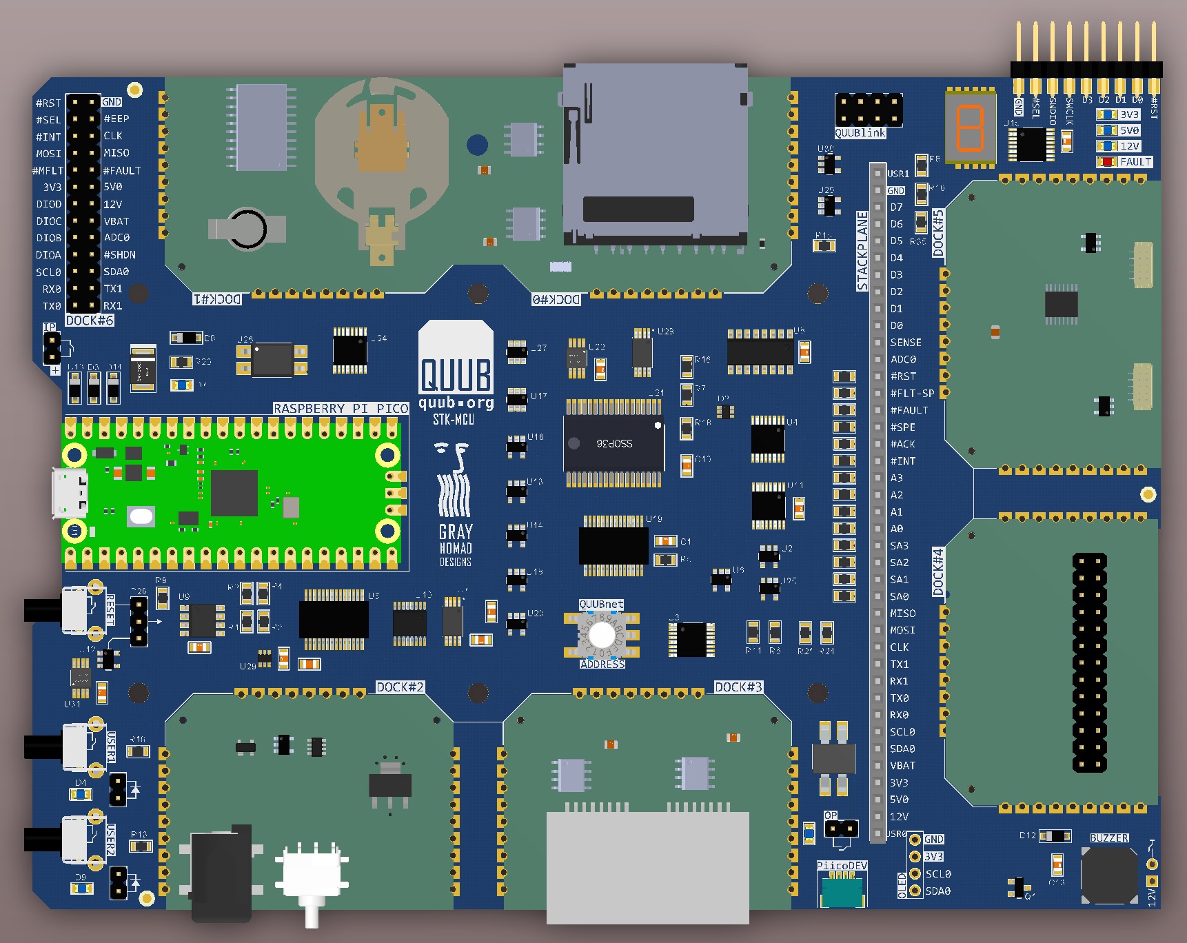
And that's where we stand today.
So why so many designs and so many years?
Well for most of those years I lived on the road in a motorhome driving around Australia and camping in remote places.
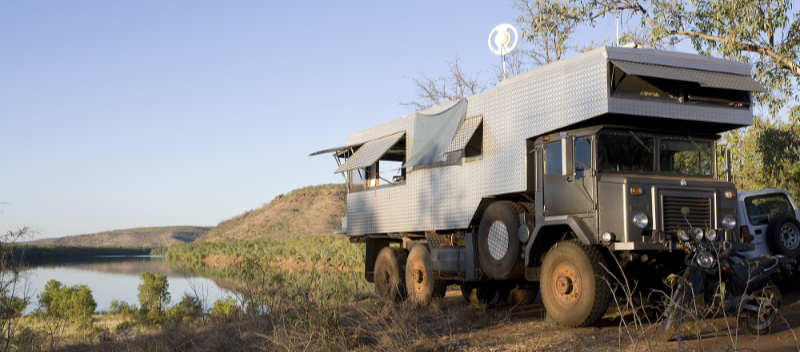
And while that environment was conducive to designing electronic schematics and PCBs and writing firmware, it was not good for building and debugging hardware.
Projects typically have four stages...
- Designing the hardware
- Debugging the hardware
- Writing the firmware
- Production
I worked in R&D most of my life. I enjoy stages 1 and 3, don't particularly mind stage 2 but wouldn't say I enjoy it, and definitely do not like stage 4.
So the QUUB is decidedly less cubish these days but I'll keep the name and as I no longer live in a motorhome — in fact I'm building a house with an electronics lab — maybe, just maybe, this version will get some legs.
|